What
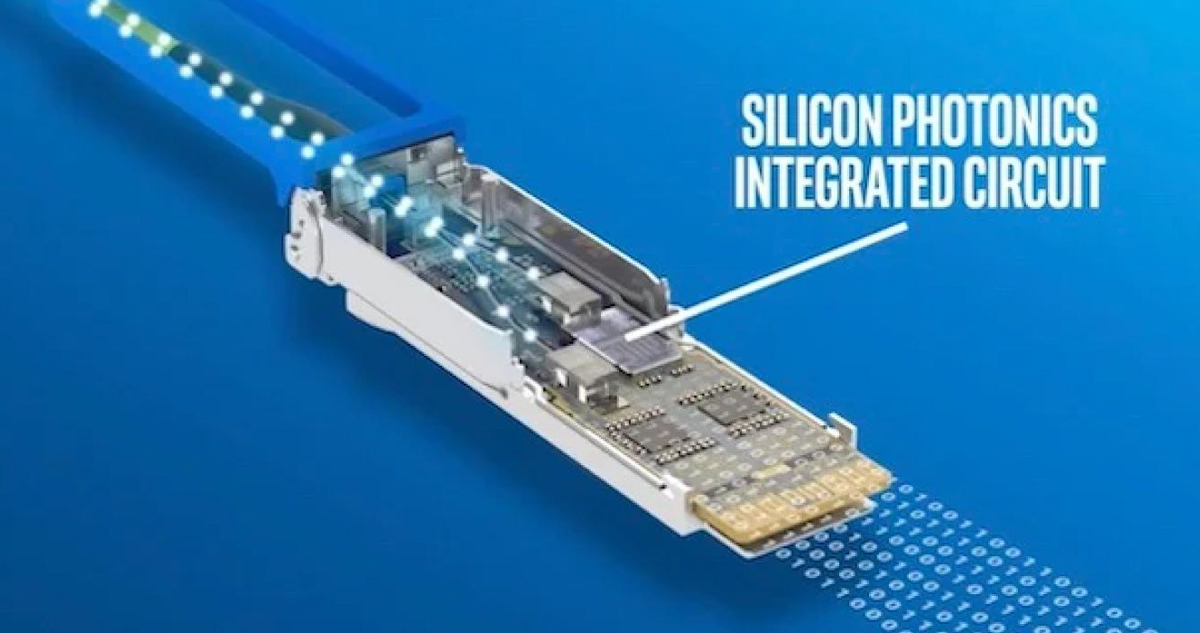
A Photonic Integrated Circuit (PIC) is a chip that contains photonic components with photons passing through optical components such as waveguides, lasers, polarisers and phase shifters. It not only performs all the tasks of the existing ICs with more precision and efficiency but has added functionality too, making it the ideal choice of manufacturers.
Why
PIC is becoming the preferred technology for data communications, Light Detection and Ranging (LiDAR) solutions for autonomous driving, sensing for aerospace and aeronautics, and more applicability with technological advancement in today’s photonics era.
PICs offer advantages such as miniaturisation, higher speed, low thermal effects, large integration capacity, and compatibility with existing processing flows that allow for high yield, volume manufacturing, and lower prices
IC and PIC
Without IC chips, it would not be possible to easily communicate over long distances and freely disseminate large amounts of information.
IC chips consist of billions of transistors for storing and processing of data, where electrical signals are used to operate them. A PIC does not rely on electrons for the operation of the circuit but uses photons which do not experience resistance in the same way that electrons do. This is beneficial for long-distance communications, where sending data via electrical means is not practical due to the resistance in the conductive material. The use of light to transmit and receive data has revolutionised the communications industry which is developing products for higher data transmission rates.
Fabrication
Ever since the IT revolution of the 80’s, the existing infrastructure evolved suiting IC manufacturing which is silicon-based. Creating a new infrastructure to suit the manufacture of PICs is time-consuming with associated cost. With more innovation, PICs capable of being manufactured in IC manufacturing infrastructure are being created, overcoming challenges such as differential heating.
PICs are fabricated using wafer-scale technology (involving lithography) on substrates (often called chips) of silicon, silica, or a nonlinear crystal material such as LiNbO3.
Testing
Testing represents most of the cost of a PIC with its outputs being consumed in all life cycle stages — from design and development, and qualification to validation and production.

MELSS brings you Test and Measurement (T&M) hardware and software solutions from market leaders EXFO, which are automated, scalable, fast, accurate and cost-optimised. These T&M solutions range from those for Passive and Active components as well as automated probe stations for wafer and single-die testing. These solutions include some of the most advanced T&M equipment such as the T200S, T500S, CTP10, CT440, OSICS T100, FTBx-2850 and OSA20.
Click here

Leave A Comment