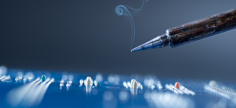
The need for soldering
Technological advancement has led to more and more miniaturisation. Millions of electronic components are packed into smaller PCBs (Printed Circuit Boards) leading to innovative televisions and mobile phones. Almost all products being used today, be it cars or rockets, rely on PCBs driving one part or the other.
Micro-components need to be mounted on the PCBs and need to be connected which is achieved through soldering. Any defect in soldering has a spiraling impact on mass-production industries such as those producing mobile phones. The soldering process has become more challenging, as with passing time it has to be accomplished in lesser space available for maneuvering on each PCB. Soldering defects are not uncommon though and need to be minimized. One of the many causes of a default in soldering is the alloy used as solder.
Classification of alloys used for soldering
The alloys used for soldering can be broadly classified into 2 types: 1) leaded and 2) non-leaded. While leaded soldering is the traditional approach, environmental and health concerns have led to the more recent non-leaded approach. Transition to non-leaded alloys for soldering is taking time and many in the field are still using the traditional approach. But technological advancement has been generating more alloys which match the leaded alloys in performance as closely as possible. Factors affecting the selection of alloys are temperature and application.
Alloy-specific issues with soldering
Non-leaded alloy usage being new, many issues have appeared in applications using it. Technological research is being done to bridge the gap. Some common defects in soldering are:
Composition: Changes in the composition of the solder alloy occurring due to prolonged heating, solder paste’s properties such as particle size, composition, melting temperature and oxide content, whiskers growing on the surface of solder alloys with high tin content (mostly lead-free solder alloys)
Usage: Cracks appearing due to mechanical and thermal stress caused by inappropriate alloy usage, solder beading error due to Inaccurate deposition of solder paste, tombstone effect caused by unequal amount of solder paste applied, defects caused by solder pads reacting with lead-free alloy with a higher tin content at a higher temperature, solder pads not being sufficiently wetted with the solder alloy
Other causes: Warping due to differing thermal expansion coefficients between the PCB and the component package, voids created due to new material base, different temperature profiles, different types of fluxes, higher surface tension of solder in lead-free soldering, voids due to 2 metals joined with different diffusion coefficients, cracks appearing due to higher temperature in lead-free soldering,
One best practice to reduce defects is to thoroughly clean the PCB after each soldering cycle.
Common types of alloys used
The most common type is a tin:lead ratio of 60:40 which is easier for cold joints and melts from 361°F/183°C to 374°F/190°C. This is very versatile as it can be applied to many applications with melting requirement within this range. It takes a few seconds to solidify after melting. Eutectic alloys which melt and solidify at the same time are used with a tin:lead ratio of 63:37. It melts at the lowest temperature of 361°F/183°C. The advantage of this alloy is that it melts and solidifies almost instantly.
Among the non-lead alloys the common ones used are tin/copper and tin/silver. Among the two, tin/copper is more widely used as it costs lesser than the tin/silver. Available ratios are tin:copper of 99.3:0.7 and tin:silver of 96.2:3.8. An alloy of tin:silver:copper of 96.5:3:0.5 is used for applications which need higher melting temperature of 422°F/217°C. An alloy that is easily available and also popular is of tin:silver in the ratio of 95:5 and this is used for audio files which need higher connectivity. This melts from 430°F/221°C to 473°F/245°C
Some solders perform better with the application of flux which is defined as percentage per cross section area of solder wire and is available as 3.3%/2.2%/1.1% flux per cross section area of solder wire. Water soluble flux is also available for specific applications.
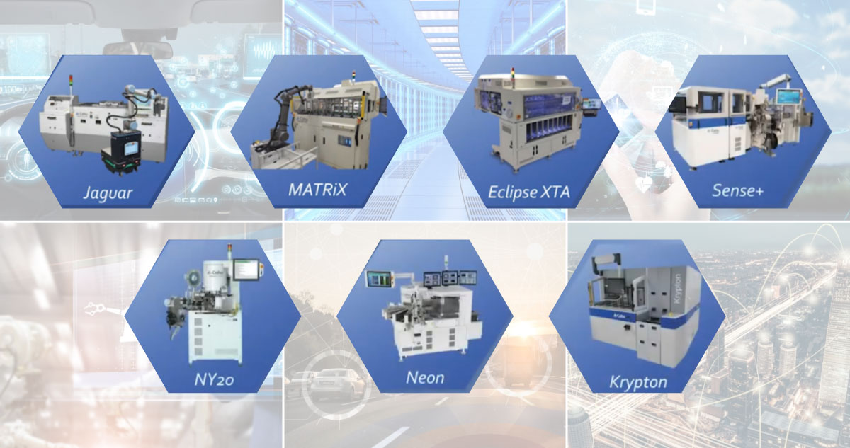
Printed Circuit Boards (PCBs) are an integral part of most solutions delivered by MELSS, and MELSS has been providing solutions for Soldering Technology for over two decades. Click here to learn more. MELSS represents Indium Corporation for their Solder Paste and Solder wires in India (Click here for a list of all MELSS partners).